
Hello all, I am back on the projects again after the traumas of moving three households into one house. Now I can perhaps have a bit of time on the workbench. The windows all open, the mice are dead and the bathrooms have been re-built. Now I want to do a little work with synthesizers. There are already a couple of synthesized projects on the homepage but I intend to do a lot more. Perhaps this is the time to do a little explaining and to introduce a couple of basic techniques and terms.
The answer to that is easy, it is a programable frequency multiplier, usually using digital logic integrated circuits. The synthesizer is aranged to multiply a reference frequency by a programable amount to achieve just about any frequency you want. If, for example you had a reference frequency of, say, 1KHz and a "programable multiplier" then you could program the multiplier to give you 1KHz (X1), 3KHz (X3), 1.025MHz (X1025), 98.325MHz (X98325) or any other frequency you want. Sounds easy? Actually, it is so easy, once you understand some of the basics. So let us start off by building a simple synthesizer that cover 3KHz to 4000KHz (4MHz).
A Phase Locked Loop (PLL) consists of a Voltage Controlled Oscillator (VCO), the output frequency of which is monitored and controlled. An error voltage steers the VCO and brings it back onto the correct frequency. The error voltage is generated by a Phase Sensitive Detector (PSD) which compares the VCO frequency with a reference frequency. Consider the following block diagram:
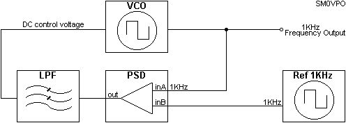
Here we have a 1KHz reference oscillator feeding the PSD Input-B, and a VCO feeding the PSD Input-A. The output of the PSD can be a square-wave and the difference between the positive pulse and the negative is averaged by the low-pass filter (LPF). This filtering results in a DC voltage that is fed back to the VCO to increase or decrease the frequency, as required.
It is interesting to note that you can put a DC voltmeter on the DC control line and watch the DC vary. The voltage will vary if either the VCO centre-frequency changes or the reference frequency changes. This circuit alone can be built using a single CD4046, but without the reference oscillator. The reference osc input can then be an external connection to make a selection of usefull instruments, such as:
The PSD signal input of the CD4046 is quite sensitive and only requires a couple of hundred millivolts of input signal to pin 14. It is DC self-biasing so all you need to do is stick a capacitor in series with your low-level input signal. For more detailled information about the CD4046 then take a look at the CD4046 Datasheet (pdf format).
Almost any logic 2-input gate can be used as a PSD, but the more usual is a simple OR- gate or an EXCLUSIVE-OR-gate. With an EXCLUSIVE-OR gate the output frequency will be twice the input frequency, but the MARK:SPACE ratio will vary as the phase between the two input signals. When the loop is "IN LOCK" there will be about 90-degrees phase difference between the two input signals. This sort of PSD is good, cheap and simple. One drawback of it is that if the two inputs are of different frequencies then the output MARK:SPACE ratio will go continuously up and down. This will restrict the ability of the loop to achieve a lock. If the natural frequency of the oscillator in the circuit above were to be less than about 750Hz or greater than about 1.35KHz then it would never achieve a lock condition. This ability to capture the VCO is measured as the top and bottom VCO frequencies that can be captured, expressed as a ratio and know as the CAPTURE RATIO. A typical capture ratio for this type of detector is just 2:1 (piss-poor) and it will even allow the loop to lock on harmonics of the VCO.
A much nicer type of PSD is composed of four Master/Slave J-K Flip-Flops in an arrangement that will deliver a permanent HIGH (1) when the reference frequency is higher than the VCO frequency. It will also deliver a permanent LOW (0) when the reference frequency is lower than the VCO frequency. When the two are equal and IN PHASE then the output may even be totally switch OFF (TRI-STATE); delivering neither a 1 or a 0 (high-impedance). This is the more usual type of PSD used in communications equipment. A typical capture ratio for a loop with this type of detector is greater than 10:1 and limited only by the practical reality of the VCO itself.
The CD4046 integrated circuit has both the above types of detector built in. The flip-flops often being used as the loop PSD and the gate can be used as an OUT OF LOCK indicator signal. Naturally, you do not want a transmitter to transmit when not locked or you have the radio equivalent of a "loose cannon on deck", so PSD II also has an output specifically for the lock detect function.
The loop filter comprises a resistor and capacitor to form a time-constant. The capacitor charges to the average DC voltage at the input and it is this voltage that controls the VCO. There may be an additional pole to the filter to help reduce the reference frequency that is sometimes referred to as "Sythesizer Whine" (even the non-English synthesisers can whine!). R1/C1 below are the basic filter time-constant and R3/C2 are the little extra filtering.
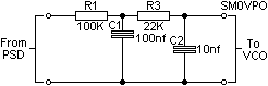
Unfortunately, with just a simple RC network, the complete PLL is a high gain closed loop with two time-dependant elements - a multivibrator! The loop will therefore never lock, but will oscillate up and down the band. Some form of DAMPING has to be included. This is shown as R2 in the circuit below.
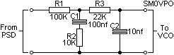
R1/C1 have a time-constant of 10mS which is enough to smooth out our 2KHz and give us a nice DC level. R2 is also added to introduce a little damping to prevent the whole loop from oscillating. R3/C2 have a much shorter time-constant and just help to clean up the loop voltage a little. The loop filter can be quite complex and is almost a complete subject in it's own right, so I do not intend to go too deeply here. The only other point I wish to discuss about loop filters is the choice of time constant.
If you were to apply Frequency Modulation (FM) to the VCO, then the time-constant shall be 5x the period of your lowest modulating frequency. That is to say, if you were to transmit HiFi music at 100MHz, then your lowest modulating frequency will be typically 20Hz. The period time is therefore 1/20 second or 50mS. The time constant of the filter must therefore be 5 x 50mS = 250mS. If not then the modulation will be seen as an error and the loop will correct it - cancel out the big bass-drum in your rendition of "Silent Night". A 250mS time constant is long, so long that it would take the loop many seconds (or minutes) to change to a new frequency. In this event you can add a "speedup" circuit that reduces the time constant if there is a large change of operating frequency.
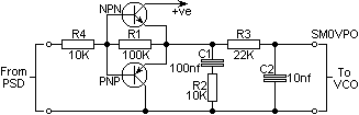
Here the two transistors operate in a complimentary push-pull arrangement, but in audio circuits they would introduce +/- 0.7v of crossover distortion. In this circuit they do not do anything at all if the loop voltage changes by less than 0.7v DC. If the loop was to be disturbed and a voltage change of more than 0.7v occurs then one or the other transistor will bypass R1, thus reducing the time constant to R4/C1.
This is usually a simple oscillator so arranged that the tuning capacitor can be varied by a varying DC voltage. This is usually done with a VARICAP (Variable Capacitance) diode. It is always well worth remembering that an RF VCO is, by definition, an "unstable oscillator". Without good mechanical stability then it will be microphonic or drift. Coils should ALWAYS be wound on formers and be well gunged up with wax, to prevent vibrations.
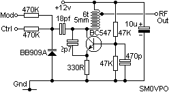
Notice how there are two inputs to feed a DC voltage to the Varicap Diode. One input would be used for the PLL control voltage and the other for a modulation input. Since the tuning diode does not draw any current a very high value of series resistor can be used (470K) to feed the DC to the diode. The rest of the oscillator is a very simple and unremarkable VHF oscillator. Those of you who have played around with my FM Wireless Microphone will no-doubt recognise the circuit. The 12pf tuning capacitor has been replaced with the tuning diode. All diodes have a variable capacitance when reverse biased and these can be pressed into service if Varicap diodes are unavailable (or too damn expensive, as they are here in Sweden). Here are a few examples of diodes that can be used:
| Diode | pf at 28v | pf at 1v | Normal component use |
|---|---|---|---|
| 1N914 | 1.8 | 3.7 | General purpose signal diode |
| 1N4148 | 1.9 | 3.6 | general switching signal diode |
| 1N4001 | 3.0 | 5.4 | 1-Ampere rectifier diode (100V) |
| 1N5401 | 7.5 | 12.3 | 3-Ampere rectifier diode (100V) |
| BZX88 21v | 4.2 | 8.1 | Zener diode (21V) |
| BB909A | 3.2 | 33.5 | A genuine VARICAP diode |
As you can see here, Zener diodes have quite a high capacitance that can be used for normal experimental synthesizer work. Be warned, the capacitance also varies with light intensity! Shine a light on them and they change a little. This could be your source of unwanted "Mains Hum" if you have flourescent lamps in the workshop. The heavy rectifier diodes also have a lower Q that could even prevent the oscillator operating with low control voltages. It is well worth noting that as the loop control voltage rises so the capacitance falls, which means that the VCO frequency will rise as the control voltage rises.
For low-frequency work you may not need VARICAP diodes at all. A simple multivibrator circuit makes a good VCO if you vary the supply voltage to the two timing resistors. A frequency ratio of 2:1 is usually possible, but the voltage to frequency sense is inverted.
The CD4046 CMOS PLL integrated circuit also has a built-in VCO that is governed by one capacitor and one resistor. An extra resistor can be used as a frequency "offset". This VCO has a range frequency range of 10:1 and will work from a few hertz to almost 4MHz.
So-far we have only considered a PLL that generates the same frequency as our reference. It could have it's uses, but let us now multiply a frequency by TEN and generate 10KHz. Consider our basic loop circuit from above, but with an added logic divider stage.
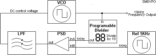
Here the output of the VCO is divided by 10 before feeding it into the PSD. This means that the loop will see an error and push the VCO frequency up until it has 1KHz at both the PSD inputs. This will only occur if the frequency before the divider is 10 times greater than the reference frequency. If you change the divide rate to 9 then the loop will only achieve a lock condition if the VCO delivers 9KHz. In other words, the divide rate multiplied by the reference frequency is equal to the VCO output frequency. If the divide rate were set to 1500 then the VCO frequency would have to be 1.5MHz. Note also that the output frequency will only vary in steps equal to the reference frequency.
The CD4059 CMOS Programable Divider IC may be set up as a Binary Coded Decimal (BCD) divider in the range of 3 to 14999. This will give you four decimal digits that you can program with DIP switches or even rotary thumb-wheel selector switches.
I do have a project on my homepages that was used to demonstrate the synthesizer principle. See my CMOS AF/RF Synthesizer (37Hz - 4MHz). Try to follow the above steps. Note that the CD4060 is a crystal reference oscillator.
Are you still with me? Easy stuff, so-far! So let's progress a little. I am sure I can complicate it all and confuse everything for you!
Yes, this is quite easy, at a simple level. As already stated, you can control the VCO frequency by adjusting the divide rate. The reference frequency multiplied by your divide rate is the output frequency. Ok then, so what happens if you vary the reference frequency? The VCO (synthesiser output) frequency will also vary. This opens up new possibilities. So let us program the divider for 1000, but instead of a crystal based reference oscillator, let us connect the CD4046 PSD signal input to a 50-ohm speaker used as a microphone, via a blocking capacitor. Place the speaker/microphone over the speaker in your computer.
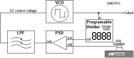
Now open the program GW-BASIC, or any other PC based BASIC language program, and enter the code listed below. Even if you are blessed with "perfect pitch" you could try whistling, but I do recommend you use your computer - it doesn't need to pause to breathe.
10 CLS: PRINT "(Gently) Hit space to end"
20 SOUND 1000,100: IF INKEY$=" " THEN GOTO 20
30 END
Now you will generate 1,000,000 Hz (1MHz) from the VCO using a 1KHz reference frequency from the computer. But if you change the BASIC program 1000 frequency value to to read 1001 you can change the reference frequency to 1001 Hertz:
10 CLS: PRINT "(Gently) Hit space to end"
20 SOUND 1001,100: IF INKEY$=" " THEN GOTO 20
30 END
You will now generate 1,001,000Hz or 1.001MHz. You can then generate radio frequency whilst controlling the synthesizer from your computer. The only snag with this method is that the sound will drive you batty. You may want to unplug the speaker in your PC and connect the synthesiser reference frequency direct to the computer. I chose not to butcher my computer, but increase the tone to 10KHz and drop the programable divider to just 100. This gave me the same 1MHz frequency, but I can vary it in 10Hz steps. I am knocking on in years and cannot really hear the tone, but it drives the cats stupid! That's Ok, I don't really want them in the shack anyway.
If you like this method then perhaps you should take a trip to my download section and use the test tone generator program GEN.EXE (zip file). Note that the frequency generated by your PC may be approximated - all due to the division of the PC's internal clock not always falling on exactly the frequency programmed, but it will always be very close.
Yes, so-far we have considered synthesisers that cover a few Hertz through to the practical limit of CMOS - about 4MHz. You could use an HEF40HCT46 PLL IC instead of the CD4046. The chip is supposed to operate at up to 15MHz, so if it is just HF you are interested in then it is time to do some experimenting. If you need to go even higher in frequency then we have to consider something else.
Those of you who have used Transistor-Transistor-Logic (TTL) will aready be aware that there are logic chips that can handle frequencies of up to 30MHz. Developments in TTL devices have resulted in "Fast TTL" that can operate at frequencies of up to 120MHz. The 74F163,for example, is a fast binary counter that can be used to make a simple synthesizer in the 100MHz range. As long as you are aware of these then you have some ideas for your own experiments. I however, will go even higher, up into the amateur 144MHz band. What we need next is a PRESCALER.
A PRECALER is a logic device to pre-divide a VHF VCO so that simple CMOS chips can be used to process the synthesizer functions. Let us begin with the SP8793 prescaler chip. This is an 8-pin device, just the same as an Operational Amplifier. The SP7893 divides by 40/41 so that a 144MHz VCO would be divided down to just 3.6MHz. This is now well within our tortoise-slow CMOS handling speeds. We take our output directly from the 144MHz VCO, but the CMOS takes it's output from the SP8793 at 3.6MHz, like this:
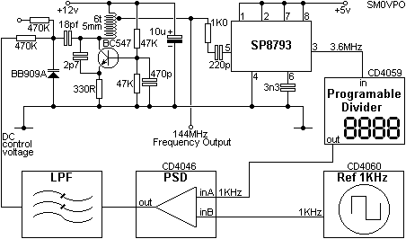
Here you can see a practical oscillator circuit operating at about 144MHz. A +6dBm output at that frequency is taken directly from the oscillator. The output is also fed into the SP8793 prescaler IC, divided by 40, then fed to the programable divider. The programable divider is set to 3600 to further divide the 3.6MHz down to 1KHz. The SP8793 prescaler is similar to TTL, but uses a slightly different technique and lower impedances. These devices are known as Emitter Coupled Logic (ECL). Much faster than TTL. I will shortly have a PCB available for this particular circuit. Note that the VCO also has a Frequency Modulation input. Notice how it is connected (470K at top left). There is no provision for deviation limiting in this circuit, that is external ano not considered in these frequency generation circuits.
The prescaler divide rate of 40 multiples the programable divider to give a total division of 144000, so you must remember to calculate your divide rate then divide by 40. This circuit also has the dissadvantage that the minimum steps you can program the final frequency in is 40KHz steps. Not very convenient! but we shall see about that later on. For the moment, we can select a different output from the reference oscillator (CD4060) to give us a reference frequency of 250Hz. So to get a final frequency of 144MHz, we need a total divide rate of 40 X 14400 which makes the numbers much more convenient (the CD4059 maximum count is 14999). This gives us possible frequency steps of 250Hz X 40 = 10KHz - much more convenient. It is certainly good enough for the local oscillator (LO) of a simple VHF FM receiver.
Are you still understanding everything? You ARE? Well we will have to do something about that!
I knew I could find something to further complicate everything. As we have seen, adding a divide-by-40 prescaler to our synthesizer we increased the minimum final frequency steps from 1KHz to 40KHz. We overcame this by further reducing the reference frequency, but this solution is not acceptable for transmitters that have to be working on frequency within a few milliseconds, or for frequency scanning and any other function that requires a fast VCO capture. So what can we do about it? The answer is DUAL MODULUS, which means having two different Prescaler divide rates.
In our synthesizer above, with the added SP8793, there are four pins all connected to the +ve 5V supply. Pin 2 is connected to set the prescaler to a divide rate of 40. If pin 2 is grounded the the SP8793 will divide by 41. In other words, the SP8793 is already a dual modulus counter, but we have not yet used it as such. Let us look at a few numbers, but we will still use our same synthesizer model with the 1KHz reference oscillator and SP8793 prescaler.
I want to synthesize 800KHz. The prescaler divides by 40, so 800 / 40 = 20. Set the programable divider to 20 and we have 800KHz. Divide by 40 twenty times. Ok - so far. So where's the problem?
Now I want 805KHz. Divide by 40 twenty times = 800KHz. Divide by 40 twenty one times = 840KHz. It doesn't work. BUT if I divide by 41 five times, then divide by 40 another 15 times I will have my 805KHz (41 + 41 + 41 + 41 + 41 + 40 + 40 + 40 + 40 + 40 + 40 + 40 + 40 + 40 + 40 + 40 + 40 + 40 + 40 + 40 = 805).
Now I want 806KHz. If I divide by 41 six times, then divide by 40 another 14 times I will have my 806KHz (41 + 41 + 41 + 41 + 41 + 41 + 40 + 40 + 40 + 40 + 40 + 40 + 40 + 40 + 40 + 40 + 40 + 40 + 40 + 40 = 806).
Clearly, we need another programable counter to control the 40/41 divide rate of the prescaler. The main counter we will call the "N-Counter" and the extra counter we will call the "A-Counter". We can engineer it with a little CMOS circuit like this:
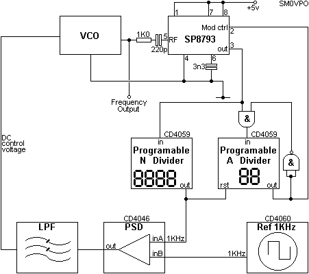
The output of the Prescaler is fed into both the N and the A counters. The N-counter is fed directly and set to the full count of 20 for our 800KHz. The A counter is set to 6, but it is fed with a signal via an AND gate. Since the output of the A-counter is 0, the inverter opens the gate for counting and the output of the counter also sets the SP8793 divide rate to 41. Now we can start counting down our 20 pulses from the prescaler, like this. Note that "Total Count" is the total divide between the VCO and the PSD.
| count | N-counter value | A-counter value |
Total count | condition |
|---|---|---|---|---|
| 00 | 20 | 6 | 0 | SET divide by 41 |
| 01 | 19 | 5 | 41 | divide by 41 |
| 02 | 18 | 4 | 82 | divide by 41 |
| 03 | 17 | 3 | 123 | divide by 41 |
| 04 | 16 | 2 | 164 | divide by 41 |
| 05 | 15 | 1 | 205 | divide by 41 |
| 06 | 14 | 0 | 246 | SET divide by 40 |
| 07 | 13 | 0 | 286 | divide by 40 |
| 08 | 12 | 0 | 326 | divide by 40 |
| 09 | 11 | 0 | 366 | divide by 40 |
| 10 | 10 | 0 | 406 | divide by 40 |
| 11 | 09 | 0 | 446 | divide by 40 |
| 12 | 08 | 0 | 486 | divide by 40 |
| 13 | 07 | 0 | 526 | divide by 40 |
| 14 | 06 | 0 | 566 | divide by 40 |
| 15 | 05 | 0 | 606 | divide by 40 |
| 16 | 04 | 0 | 646 | divide by 40 |
| 17 | 03 | 0 | 686 | divide by 40 |
| 18 | 02 | 0 | 726 | divide by 40 |
| 19 | 01 | 0 | 766 | divide by 40 |
| 20 | 00 | 0 | 806 | All counters reset |
The contents of the A-counter is ZERO after the 6th pulse and so the output changes state. This changes the modulus control to the prescaler from 0 to 1 as well as closing the AND gate, so preventing the A-counter from doing anymore counting, until the N-counter has finished. As you can see in the fourth column, the total count is now 806 which will set the VCO to 806KHz using a 1KHz reference oscillator.
So, to program a "dual-modulus" synthesizer:
You may wish to experiment with synthesizers and heaps of CMOS, but today there are loads of chips already on the market, such as the MC145152-2 which has built in A and N counters as well as all the necessary support logic. If you want more information about this family of chips then you can download the mc145151.pdf family datasheet, which shows the MC14151 single modulus, MC14152 dual modulus, and other sysnthesizer chips in that family.
Are you STILL with me? Did you understand all that?? Ok then, you asked for it!
So-far, we have only considered synthesizers that have loads of wires to which we can connect a load of switches, diode matrixes or splashes of solder, to program. These are all called Parallel Load synthesizers. They are great for the hobyist, but when it comes to interfacing with microprocessors there are just too many wires to handle. Besides that, most radio and communications equipment processors output the data in serial format anyway. This means that there are loads of synthesizer chips on the market designed for car radios and communications stuff. They usually have a minumum of a 1.1GHz prescaler built into the chip. To use these chips you only need an external crystal and a VCO, the rest is done internally. These are termed Serial Load synthesizers.
Let us take the example of the MC145158 "Serial-Input PLL Frequency Synthesizer". Let us assume you have already connected your crystal, VCO and prescaler as per the data sheet and are now ready to program it. This chip has three registers to which you have to send data:
| 14-BIT R-COUNTER | Divides the crystal to give you your desired reference frequency. For example, if you wanted a 6.25KHz reference, then you could use a 12.8MHz crystal and set this register to 2048. |
| 7-BIT A-COUNTER | Sets the value in the A-counter in exactly the same way as we have done in our dual modulus example in this article. Leave this set to ZERO if you want single modulus. |
| 7-BIT N-COUNTER | Sets the contents of the N-Counter in exactly the same way as all the examples in this article, both single and dual modulus. |
You send to the chip the R-Counter value in serial binary format to the DATA input pin, begining with the most-significant binary digit. When each data bit has been presented, just clock the CLK pin high, then low to advance to the next bit of data. When all 14 bits have been sent, you set the last bit to 1 and clock it again. This will set the R-Counter with the data from the shift register. To program the A and N-Counters you sent the 7-bits of the N-Counter (MSB first) then the 7-bits of the A-Counter (MSB first) then follow it with a 0. Again you pulse the CLK input to store each bit into the chip. The 15th bit (0) tells the chip it is not an R-Counter digit.
At this point the synthesizer chip is still working on the old frequency data and will continue to do so until you send a pulse to the ENABLE (ENB) input of the chip. At this point the synthesizer will change to the new frequency program. You can therefore pre-load the synthesizer with your transmit frequency whilst still receiving. On TX key you just hit the ENB with a pulse and you are on the TX frequency. Your logic should then pre-load the RX frequency again waiting for you to release the TX. All this information is contained in the MC14151 datasheet.
I hope that you leave learned something and have fun with this information. Very best regards from Harry - SM0VPO
Return to INFO page