
Introduction
It was only a few years ago that you could buy those more exotic chips to build radio frequency synthesisers. My particular favourite was the MC145152-2 that could be programmed with DIP switches, a diode matrix, or even a pair of EPROM look-up tables. But sadly, those days are over. The MC145152-2 costs about US$30, if you can find a supplier. Today we need to use PIC-processors to program modern synthesiser chips, or have them permanently connected to a computer. Todays synthesisers are becoming more and more surface-mounted. Whatever happened to the bits that the hobbyist can actually use?
What I want is a synthesiser I can use. I want it accessible. I want to be able to use diodes or solder-blobs for programming. I want just "throw together" a slack-handfull of bits and make a working synthesiser, without having to take a course in yet another processor. With these thoughts in mind I devised this project. It uses three different "bog-standard" CD4000 series CMOS chips, and not the hard-to-get ones, either. Have you ever tried to find a CD4059B recently?
A basic CMOS synthesiser is already on my homepages, based on the CD4046B. It can work up to about 3.5MHz, but it is only meant to demonstrate the synthesiser principles. If you add a bit more care to the filtering then there is no reason why you cannot use it for communications. But let us now re-design that project, using easy-to-get CMOS, and add dual modulus (swallow counter) operation. Too good to be true? Read on.
Synthesiser Recap
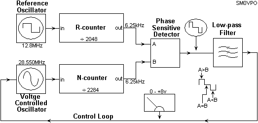
Here is the block diagram of a basic synthesiser. The "R-counter" generates the reference frequency. In the MC145152-2 you have about 3 different options. In mine you will have over 2000 different options. The reference frequency can be interpreted as the channel-spacing of the final synthesiser. The "N-counter" divides the output of the external voltage-controlled oscillator (VCO). The output of the N-counter is compared with the reference frequency, and the different is the error signal that is used to control the VCO.
In principle, the synthesiser is a frequency multiplier. It multiplies a reference frequency by a "N"-counter program.
For example, to synthesise 125kHz you can use a reference frequency of 5kHz and an N-counter program of 25 (25 x 5kHz = 125kHz).
My own CMOS synthesiser project is great up to 4MHz with the CD4046B chip, or with an external VCO up to about 30MHz, which is about the limit for CMOS. If you had a reference frequency of 12.5kHz, then divide the wanted frequency (eg. 28.550MHz) by the reference frequency and you get the N-count. 28.550MHz / 12.5kHz = 2284. Change the program from 2284 to 2285 and you will get 28.5625MHz.
The basic problems arise when you want to build, say, a 145MHz synthesiser. 145MHz is out of the range of the CMOS, so a prescaler is used. But with a prescaler that divides by 32, you need to have a reference frequency of just over 390Hz if you want to get your 12.5kHz steps. The loop also needs to be filtered so much that a change of frequency will take many seconds, instead of a couple of milli-seconds. The previous example frequency of 28.550MHz, when used with a /32 prescaler would need a divide rate of 71.375 = not possible. What is needed is a "dual modulus" prescaler.
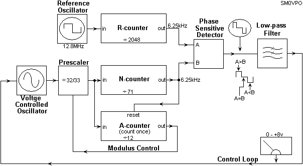
Point of interest here: a divide with a fixed "count" is refered to as a "fixed modulus" or "single modulus" counter. Modulus is singular. It should become a "dual-moduli" counter in the plural form, but engineers are never very good at languages that cannot be expressed in "1"s and "0"s.
The MC145152-2 also has an "A-counter". The A-counter, sometimes called a "Swallow counter", works in tandem with the N-counter to change the divide-rate of a prescaler. By changing the prescaller to divide by 33 for a few cycles, then by 32, you can extend the count to fill in the gaps to get your 12.5kHz steps again. To do this you need another counter - the A-counter. In the 28.550MHz example, with a divide-by 64 prescaler and a 12.5kHz reference, you would use an N-count set to 71 (71 x 32 = 2272), and put the missing 12 counts (2284 - 2272 = 12) into the new A-counter.
Let us now take a closer look at the timing. But for the sake of simplicity I will reduce the numbers a bit. Let us assume I want to generate 4456.25kHz and the prescaler is a divide by 32/33. I will keep the reference frequency of 6.25kHz, so 4456.25kHz / 6.25kHz = 713. Using a /32 prescaler I have an N-count of 713 / 32 = 22 but with 9 left over for the A-counter. Pretend I have just built it, it works, and now we shall look at the timing diagram. Study the block diagram, the waveforms and the description in Table 1 until you understand it.
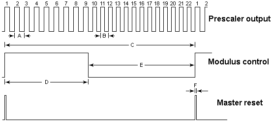
| Pulse | Waveform description | Duration |
|---|---|---|
| -A- | This is 4456.25kHz divided 33 (slow prescaler count) | 7.40us |
| -B- | This is 4456.25kHz divided 32 (fast prescaler count) | 7.18us |
| -C- | 22 pulses (N-count) 4456.25kHz divided 713 (9 x 33 + 13 x 32) | 160us |
| -D- | 9 pulses (A-count) 4456.25kHz divided 9 x 33 | 67us |
| -E- | 13 pulses (N-A count) 4456.25kHz divided 13 x 33 | 93us |
| -F- | 6.25kHz, pulse duration = 2 x CD4001 gates delay (exagerated) | 0.05us |
As you can see, the prescaler divides by 33 for the first 9 output pulses, then waveform DE changes from high to low, to tell it to divide by 32 for the remaining 13 counts. This is what I want to achieve, but using normal, readily available CMOS chips that you can buy from your local electronics shop.
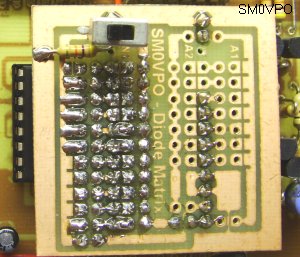
The Diode-Counter Technique
Now I shall introduce my somple diode counter. To start off with, the MC145152-2 A-counter can have a count of 512, 1024, or 2048. This means that a 12.8MHz crystal, divided by 1024, will give you a reference frequency of 12.5kHz. You could alternatively use 6.4MHz divided by 512. Not many options there! You still need to buy a special crystal.
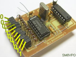
In my counter you can divide by ANY number from 2 to 2047. I put my hand in my junk-box and fished out a 5075kHz crystal. I can get 25kHz from that by dividing by 203. Of course, I can also adjust the oscillator a little if the frequency is not exact. 203 (decimal) is 11001011 in binary. Add leading zeros to get 11 digits, and we have a binary count of 00011001011. Each "1" is a link you put into this circuit:
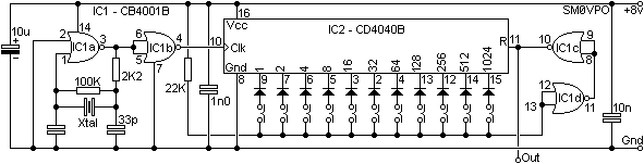
IC1 is a CD4001B, quad NOR gates. IC1a is the crystal oscillator, but you can add a few turns of wire to pull the crystal a few kHz. You can also increase the 33pf capacitors to drag the frequency down a bit. The capacitor connected to the 100K/2K2 junction can be increased to 100pf, if necessary. You can also add a small inductor in series with the crystal. IC1b is just a buffer.
The 22K resistor is a pull-up to Vcc (+8v) and is coupled to the Reset (R) input of the counter. The counter delivers a binary output from 12 pins, but I have only used eleven of them. If any output has a logic "0" (low voltage) then this will sink the bottom end of the 22K resistor to ground, through its respective diode. If you pull out a link, then that output can be forgotten: it is only the "1"s that count. If the binary 00000001011 were programmed, then the 22K will not pull up to +8v until the count reaches 11 (decimal) (000000 + 8 + 0 + 2 + 1 = 11). In this photograph I have programmed 203 (00011001011).
The 22K is not connected directly to the counter reset input. The capacitance of the PCB, and the 22K resistor make this pulse a rising sawtooth, with a rapid return to ground. The pulse would be far too short to feed any external circuits, so I have added and "IS" gate (two series-connected "NOT" gates), (or if NAND is to AND, then NOT should be an OT gate ... Duh! Oh forget it). The transition delay of these gates ensures that a nice pulse of a few nano-seconds resets the counter, and the pulse is long enough to ensure that successive CMOS circuits are also clocked.
Notice how I fit the unused links to the left, sitting on just one post. That way all the links available for future use.
This circuit will later be used as the heart of my synthesiser, but it demonstrates how to make a divide-by-N stage using normal un-sexy, garden-variety CMOS. You can use this to generate 1750Hz to access repeater, using any-old-crystal. To get a near 1:1 mark-space ratio then take your output from the last (most significant) diode anode that has a link fitted. Use a 32,768Hz clock crystal to get any other frequency you like.
A PCB foil pattern and component overlay is given on my homepages. It is a ZIP file containing information (in English), and 250 pixels/inch BMP files.
The Double Diode-Counter Technique
Text books and school diagrams, as in figure 2, all show the N-counter and A-counter as two seperate counters. In practice they can be the same counter, if you expand my CMOS counter technique a little. I will use that cheap CD4040B counter again, but this time I will use two diode matrices:
The first diode matrix resets the counter, exactly as I showed in the previous sub-project. The second matrix detects the A-count, and sets a latch. The Q output of the latch will change low-to high when the A-count has been reached. The NOT-Q output is the one we want. It will be used to set the prescaler "Modulus Control" line to "1" so the count is 33. After the A-count has been reached the NOT-Q output will change to "0" and set the prescaler back to divide by 32, and stay that way until the N-counter has been reset.
At first glance, a basic problem with my CMOS/Diode counter technique is that the program count will be detected several times. A count of 18 (00000010010) for example, will also occur at 00000110010, 00001010010, 00001110010, 00010010010, and so on. In this application this does not matter. No matter how many times you "set" a latch, it will only continue to do what it is already doing. We only need detect the first occurence of xxxxxx10010, where x = don�t care.
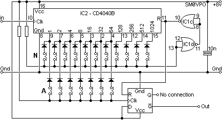
Here is a practical circuit of the A and N counters, using cheap CMOS and a heap of diodes. The "Out" pin is the Modulus Control pin to the prescaler chip. The A count can never equal or exceed the N count, and should never exceed the divide rate of the prescaler. So I have only used seven diodes, which allows an A count of up to 127. This should just about cover all the prescalers chips that are left in the market place. I will use an MB501 (SA701, SP8704, MC12022), which can be set to 64/65 or 128/129. The chip will also work up to 1100MHz, so this synthsiser card will suit just about all your requirements. I will translate this circuit to use actual components and pin numbers, as they will appear on the main PCB, but first, let us look at the loop filter.
Loop Filter
This is where many amateur synthesiser designs fall down. Basically the output of the Phase Detector in the CD4046 (pin 13) has a 47K and 0.5uf capacitor as smoothing. The smoothed output across the 0.5uf cap is not used because the two transistors are turned OFF (the loop needs to change level by more than 0.7v before either of them turn on). Next there is a 47K + 50nf and another 47K + 50nf which form a 2-pole filter. This gives a nice low-pass filter and stops ripple at more than 5kHz. It has a 6dB/octave roll-off.
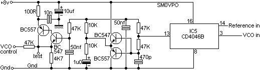
In the event the loop suddenly goes out-of lock, the voltage across the 0.5uf changes by more than 0.7v and causes one or other of the two transistors to conduct. The 10K + 1uf at the emitters of the transistors will suddenly change, and a 10K feed into the loop bypasses half the loop filter. This allows a very rapid frequency change, for example when you change channel, but under normal circumstances the 47K - 2x 10K and 1uf will follow small drift changes and keep the loop in lock.
Long time-constant when in lock, but short time-constant with dramatic change.
Overall, the loop will filter out audio changes, above 300Hz, so the loop will not see modulation as an error. Frequencies below 300Hz will pass through the filter and be seen as an error. Frequencies above 3.5kHz will be removed, so preventing that synthesiser "whine". As long as the reference frequency is 5kHz to 25kHz. The ideal is 6.25kHz, so two counts equal one NBFM channel.
The last two transistors, to the left in the diagram, form a simple a DC buffer. It is an NPN emitter-follower, BUT the transistor is bypassed by a PNP transistor, just as you sometimes see in high current voltage regualtor circuits. This has the effect of increasing the input impedance of the NPN transistor to many Megohms, so it does not change the properties of the filter, or put a resistive load on the filter output. I could have used an IC here, but the original object was to keep it simple.
Modulation should be applied to a second diode in the VCO.
So now you have the reference counter, the N counter, the swallow counter, and the filter. The diode matrices for the A and N counters are fitted to a seperate plug-in board, and the VCO and prescaler is fitted to an external VCO daughter board. My motherboard also has a CD4046 CMOS PLL chip. You can link the VCO in the CD4046 to use the on-board VCO and build a synthesiser for up to about 4MHz. Use the external VCO and you can go up to 1200MHz, using prescalers. To enable the on-board VCO add a solder-blob in the PCB copper side under the CD4046, as shown below.Putting It All Together

There is a dedicated "enable" pin on the CD4046 (pin 5), but I chose to enable the output circuit using a solder-bridge because I want as little load on the external VCO as possible. All that is missing now is the complete circuit of the final circuit board. Take a long look at this:
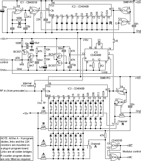
| IC Components List | ||
|---|---|---|
| Component | Value | Comments |
| IC1 | CD4001B | Quad dual I/P NOR - CD4011 also works if pin 2 = Vcc |
| IC2 | CD4040B | 12-stage ripple counter |
| IC3 | CD4040B | 12-stage ripple counter |
| IC4 | CD4001B | Quad dual I/P NOR |
| IC5 | CD4046B | CMOS PLL. Do NOT use 74HEF4046. Stick to the common simple one |
| IC6 | 78L10 | 1A 10v positive regulator. IC6 not shown. |
There needs to be some explanation here. The "Internal VCO Select" is a wire link on the PCB. Do not fit this link if you want to an external VCO. Instead fit the link to the external VCO on the board. R1, R2, and C1 are the resistors used in the VCO timing circuit of the on-board VCO, see the CD4046B datasheet for details. In principle, one resistor works with C1 to determine the frequency. The other resistor is an offset to limit the frequency range. The "VE" link can be removed to disable the on-board VCO. For up to 2MHz C1 is 47pf and R1 (4046 pin 11) is 10K. Change C1 to 22pf and you can program up to 4MHz.
The terminhal marked MC changes the divide rate of the prescaler. This pin is always high (logic "1") when the count cycle starts, but after the A-count has been reached it goes low and stays low. This would change your prescaler from divide by 65 to 64, or 129 to 128, etc. After the N-count has been reached, the counters are all set to zero, the MC becomes high again and it all repeats. One small point, most prescalers have a +5v Vcc, and the MC line should be the same. You can use a simple resistive voltage divider to do this, or use a resistor and a diode clamp to the +5v prescaler supply.
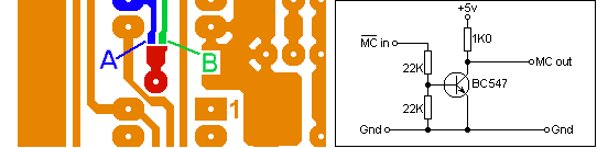
On the mother card I have added a couple of solder links. The first of these is the Modulus Control (MC) as shown above. For normal positive logic you should blob the pad "A" (red to blue). This will configure the modulus-control line to logic "1" on reset, but return to "0" when the A-count has been reached. The basic problem is that this board uses a 10v supply and most prescaler chips need 5v logic. An elegant solution is to use a simple transistor as a logic level converter. Unfortunately this will reverse the sense of the MC signal. In this event you can alternatively solder-blob the "B" link to get an inverted MC signal.
The CD4046 also has an internal phase detector. My diode-counter technique only delivers minute pulses, but the PSD-II in the CD4046 can easily cope with this to give a true HI/Lo/Tristate output with frequency/phase difference. It uses dual master-slave J-K flip-flops so it does not lock on harmonics. The two inputs are pins 3 and 14, with 14 being the reference frequency input. A normal VCO has a positive transfer function - as the voltage rises, so does the frequency. You can measure the LOOP voltage at the point marked "test". The VCO centre frequency should occur when this voltage is 4.0v.
I had thought of using diodes to combine the pulses from each diode matrix, then just apply volts to whichever 22K channel you want. This did not work. At 5MHz the whole synthesiser is running close to practical limits of board capacitances. In the end I said "sod it!" and put in a switch. The switch selects channel 1 or channel 2. There are two switches, one for the N-counter and the other for the A-counter. If you want more than two channels then plug in a different diode matrix board.
This circuit is really quite simple, but the complexity happened when I put it all together on one board. The A and N diode banks and the four 22K resistors have become 10K, plus four extra diodes and two 47K resistors. All these are all mounted on the extra board. I will now work on that while you try to make sense of this circuit. I must confess that it was a bit of a head-scratcher, with so many tracks to follow simultaneously.
Please note that I have sprinkled a few extra decoupling capacitors across the 10v supply, close to the ICs. These are not all documented in the circuit. If you really want to document them then download the PCB foil and overlay (when I have finished them), and count them. Please also note that at this moment I have laid out the board after the rats-nest sitting on my workbench. There could be wiring errors, but I have tried to get it all as accurate as possible. I will update this project again when I have built the final PCB, but the project is documented here for you to play with. Call it a "Beta release 2", :-) Yes, I like that! If it's good enough for Micro$oft, its good enough for me.
In recent weeks I have become a lot more active on the HF bands. I have ordered a few hundred QSL cards, and started operating PSK-31. Lovely mode. The only problem is that my old Yaesu FT-101ZD has a valve PA, and is based on a 5-5.5MHz VFO. This makes it unsuitable for PSK-31, unless you wish to inflict your frequency drift on the other guy. An alternative to this is to feed an external signal into the external VFO input. The external VFO can be my synthesiser prototype. It works! So here is my VFO covering 5MHz to 5.5MHz.VCO for MF-HF-VHF
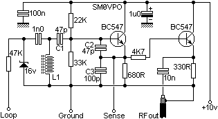
It is a simple Colpits oscillator, but it has a 78L05 5v regulator (not shown) as the supply feed. The 22K and 33K resistors bias TR1 emitter to about 3v DC, which means that TR1 emitter can feed the CD4040 counter input directly when the synth is fed from a 10 volt supply. This is the "sense" output. TR2 is a buffer with an additional 4K7 base feed resistor to further buffer the oscillator from the output stage. The output from TR2 emitter is about +10dBm.
L1 determines the frequency and you need change this component, plus a few caps, for other frequencies. This circuit will cover from 500kHz to 15MHz with nothing more than component changes. L1 was wound on one of those surplus RF coils for PCB mounting, but a "recovered" transistor IF can is the same thing. Carefully remove the existing wire and wind a new coil, and change the capacitors, according to the following table:
| Freq | L1 (turns) | C1 and C2 (pf) | C3 (pf) |
|---|---|---|---|
| 500kHz | 400 | 470 | 1000 |
| 1MHz | 200 | 220 | 470 |
| 2MHz | 100 | 100 | 220 |
| 3MHz | 70 | 68 | 150 |
| 4MHz | 50 | 56 | 120 |
| 5MHz | 40 | 47 | 100 |
| 6MHz | 30 | 39 | 82 |
| 8MHz | 25 | 33 | 68 |
| 10MHz | 20 | 27 | 56 |
| 15MHz | 12 | 18 | 39 |
Note that these values are given as a guideline only and may vary quite a lot, depending upon the coil formers you use. The trick is to wind one coil, fit the caps and then measure the frequency. You can usually just adjust L1. But if the frequency was, say 20% too high, then increase L1 turns and capacitor values by 20%. Easy! My figures were tested at 1MHz and 5MHz. I used L1=35 turns, C1=47pf, C2=47pf, and C3=100pf. This gave me 5MHz to 5.5MHz by setting the ferrite slug.
For the Yaesu FT-101ZD a VFO tuning 5.5MHz to 5.0MHz tunes 3.5MHz to 4.0MHz, but there is a slight offset. For PSK-31 on 3.580MHz I need a VFO frequency of 5.419MHz. Using 6.25kHz reference oscillator I got close, but a few kHz too high (VFO too low). So I put a 15pf capacitor in series with the 5000kHz reference crystal on the synthesiser board, to push the reference frequency up a bit. This now gives me exactly the right frequency for PSK-31 on 3.5MHz. Where there's a will there's a way!. You can make slight frequency changes to the crystal to get precise calibration.
There is only one small "bug" with this FT-101ZD solution - 4.5MHz is about the highest frequency sinewave you can put into the main board. In order to get 5.5MHz I had to take the board supply up to 12.5v DC to get it to count the oscillator. If you do this with the HEF4040 then it will dissapear in a puff of smoke. CD4040B works fine and well within its tolerances.
On the main board reference oscillator section, there are two capacitors in the reference oscillator section: "C+" and "C-". Under normal circumstances these are not fitted, and in place of "C+" is a wire shorting link. But if you want to "trim" the complete synthesiser you can do this by fitting capacitors. "C+" increases the reference. The smaller the capacitor so the higher is the frequency. Value as low as 12pf can be used. "C-" lowers the refrence frequency. The larger the capacitor so the lower is the frequency. You can fit up to 150pf here. This should be done with reference to a frequency standard, such as WWV on 5MHz.
This VFO shows you the principle involved for other VCOs, with or without a prescaler. The only thing you have to remember is that the synthesiser board uses a 10v supply, but 5v prescaler chips use 5v logic. You need some sort of logic level converter. I used two resistors in my prototype, but a transistor level converter would be more elegant, and faster, as detailled in the section "Putting It All Together".
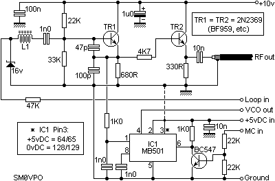
The above circuit is perfect for VHF use, up to about 450MHz. It has a very wide frequency ratio. TR1 and TR2 can be BF959 for frequencies above 200MHz, 2N2369 for frequencies above 60MHz, and BC547 for frequencies below 30MHz. I must stress that this circuit is a suggestions and has only been built on a "rats nest" board, but there is as yet no PCB available for it. "Point-to-point" wiring on copper-clad board is probably the best construction method for frequencies above 30MHz. Typical values for L1 using 0.15mm Dia. enamelled magnet wire on a 5mm Dia. air-dielectric former are: 50MHz 30-turns, 75MHz = 28-turns, 145MHz = 5-turns, and 300MHz = 1.5-turns. For 450MHz L1 should be about 1/2 turn, 12mm Dia. using 0.5mm Dia. wire.
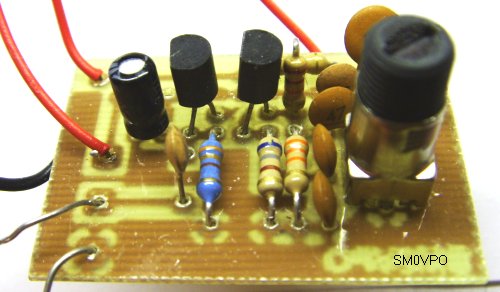
I have already finished the updated synthesiser card and it is available for download. The PCB is to be found on my download site as a single ZIP file, filename = "4040_divider_pcb-files.zip". All my PCB drawings are drawn in BMP, 2-colour, with 250 pixels per inch. This is what the finished main board looks like:Epilogue
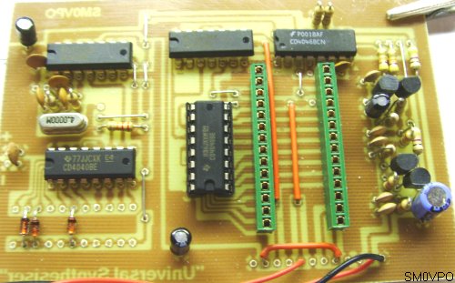
In this version I chose a 4.000MHz reference crystal, so I only need to fit the diodes in (right-to-left) /32, /256, and /512. So the divide rate is 512 + 256 + 32 = 800, so I get a 5kHz frequency reference when 4000kHz is divided by 800.
Remember that for the FT-101ZD I did not use dual modulus, so the two /A banks of diodes are not fitted. I fitted the two /N banks so I could select 5360kHz (for 10.140MHz), and 5430kHz (for 14.070MHz). The switch selects which diode matrix bank I want to use.
I will probably add more modules as and when I have the time, so please bear with me. But now you have the PCBs and VCOs I consider this project to be finished, but with a future VHF/prescaler board and EPROM lookup to be added, as and when I have the time. The matrix board has been added to the file, but I may look into the possibility of using two EPROM memories to make a huge channel-table. No promisses, though.
One small but interesting point, do NOT use dual modulus for WBFM. A VCO intended for music should have a good response at 10Hz modulation, and the loop filter capacitors all must be increased by at least 10x. Because of the wide deviation, the output of a prescaler will vary by much more than one radian, which means that a phase lock is never possible. The CD4046 detector will allow a "frequency lock", but the MC line would become somewhat eratic, causing bad modulation.
I must also comment upon one person who recently wrote to me to ask if I would add a version of the PCB with thumb-wheel switches. I said "no, not enough time, and it is outside the project scope". The e-mail reply was "Not acceptable!". This is the reason I often state that this project is only a hobby, which commands a much lower priority than Maj-Lis, the house, work, sickness, etc. If I want to operate my HF radio then I shall do that. I wanted to develop this project further, which is why you are able to read this text now :-)
Whatever you do, have fun. Very best regards from Harry - SM0VPO