
I am unable to use packet radio here in Sweden because a SYSOP will not allow me to use FBB software for a PMS system. As a result all mail to and from me is deleted. The solution is quite simple, log on to a BBS in another country via HF where they know how to set up a packet system. That was the motive behind this project but you can use it for a load of things, for example:
So why is this project so versatile? First of all it has two different inputs, one for 600Hz FSK and one for keying the oscillator. It is based upon a crystal so the HF stability is excellent. With an on-board inductor you can move the carrier up and down the band by about 3KHz or so and it will work on the fundamental of any crystal from 1.8MHz to 20MHz. Incidentally, it can also be driven with the BAYCOM software for use on packet.
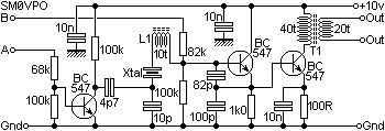
The card is fairly straight forward with TR2 as a crystal controlled oscillator and TR3 as the output buffer amplifers. The output power is in the region of 100mW. Incidentally, 100mW can get you many kilometers since it is quite possible to work 1,000,000 miles (1,600,000 Km) per watt under ideal conditions. You would need an output low-pass filter since the signal generated is quite rich in harmonics.


To the left you can see a 14MHz carrier using a 1MHz spread (13.5MHz - 14.5MHz). It is exceptionally clean but when you look at the right-hand trace (DC - 60MHz) you can see that the harmonics are quite well defined. The second harmonic is the largest but this is some 14dB down on the fundamental. A simple low-pass filter with a cut-off above 15MHz is all that will be needed to clean up this oscillator if it is to be used as (or the heart of) a transmitter.
The oscillator uses L1 in series with the crystal to pull the frequency quite a bit. The small value series capacitor pulls the crystal back up again. This means the crystal can now be pulled over a reasonable range of several kilohertz. Transistor TR1 collector has a high-impedance load (100K) but when TR1 is made to conduct the collector circuit becomes low impedance. This has been used to add 4p7 to the oscillator tuning capacitance so that FSK can be generated by applying a positive signal to the input A. A positive signal must be applied to the B input to make the oscillator start. If you wanted to have two separate oscillators, one for Tx and another for RX then build the second using BC557 transistors instead of BC547. The B input will then need to be grounded to start the oscillator. Both oscillators can then be keyed from the same source.
The output transformer T1 is wound on a 1/2" Dia. ferrite ring. Primary is 40 turns and the seccondary is 20 turns. A simple method of winding is to take three lengths of No 30 SWG enamelled wire (pretty thin) each about 1 meter long. Twist them together to make a 1 metre long three-core wire. Now wind 20 turns on the ferrite ring. Using an ohm-meter identify the start and end of each of the three windings (A1 A2 B1 B2 C1 C2). C1 and C2 connect to the output terminals of the board. Connect A2 and B1 together. Connect A1 and B2 to the amplifier stage TR3 and supply.
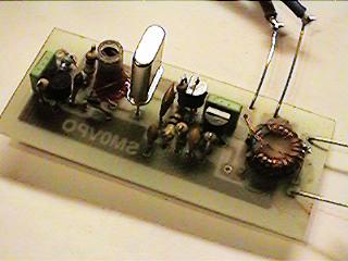
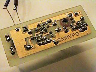
Here is the finished prototype. The crystal is left hanging because it is a 14MHz test crystal. I really need a 14.1MHz crystal for my final project. If you have got four of them to spare then please give me a call. A PCB and component foil pattern are available and they can be downloaded via my INDEX page.
Have fun, de HARRY, Lunda, Sweden.