
Here is an interesting little project. It is not exactly 100% finished, but here is a working example for you to play about with. As you may be aware, I have been rather kinky about DC/AC converters (inverters), and this is yet another example of the same thing, but with a little twist.
Since I shall shortly be unemployed, I though I should update my knowledge and teach myself the art of PIC programming. Maj-Lis bought me a starter kit for Christmas (2009) and on the 01st of February 2010 I started to read through the "gumph". I put the all-singing, all-dancing 16F690 chip back in the box and bought myself a few lesser-complicated 12F509 chips. They cost about US$4 each (including postage and stuff), have 1kBytes available for program memory, and have an in-built clock. They are also easier for "old codgers" like me to learn :-)
I wanted to produce my first DC/AC converter that gives a "modified sinewave output. This I have achieved. This project will deliver about 30 Watts at 230v AC (115v AC). Please note that the actual voltage peaks are now about 50 Volts higher (25V in 115v system), just like the "real" mains utility outlet. This is adequate for powering these low-power economy lamps, or mobile phone chargers, from your 12v vehicle battery.
This project is the result of the last three weeks (on and off) learning, in between the hysterical job-hunting frenzy. Please forgive me if I made any errors.
The 12F509 is ridiculously easy to learn and perfect for beginners. It has an internal 4MHz oscillator, which means you do not need to provide this on the PCB. The oscillator is of the R/C type, but the chip comes with a pre-programmed calibration byte, so absolutely no external clock circuitry is needed, and the accuracy is better than +/-1%.
The processor chip has two supply pins (1 and 8), and all the other 6 pins are I/O lines. I have chosen to use GP0 and GP1 (pins 7 and 6 respectively) to give two anti-phase signals to control the power transistors. The processors maximum supply voltage is 5v DC, so there is not quite enough to drive a MOSFET hard enough to minimum resistance, so four push-pull transistors have been used to drive the Gates of the power transistors.
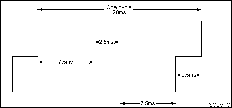
Four MOSFET power transistors have been used in push-pull, two N-channel and two P-channel, to provide switched power to the 9v-230v (115v) power transformer. The output is a square-wave, but with a period of neither positive, nor negative. It is for this reason that a 9v transoformer is used, instead of a 12v transformer. The timing diagram looks something like this:
Note that in the software I just used "7" and "2" in the descriptions. If you read the source code then remember that my comments are shortened and cryptic, jst lke prfesnal cmpter prgrmrs. Bt I gess u cn rd mi cmnts wtht prblm :-)
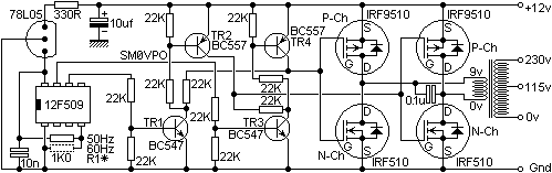
The heart of the circuit is a 78L05 5v regulator, powering a 12F509 processor. The traditional 10nf (0.01uf) cap is used to decouple the supply. I have added a 330 Ohm resistor in the supply line to the regulator. This resistor allows you to use a 24v nominal (29v in reality) power supply without exceeding the regulators voltage specifications. It also burns some power, instead of forcing the 78L05 to do the burning. The regulator in the diagram is viewed from above.
The processor (viewed from above) has 5v DC power applied to pin 8, with pin 1 to ground. Pins 6 and 7 are the output pins. Pin 4 is a "special". The 1K0 resistor is fieed in only one position, depending upon whether you want 50Hz or 60Hz output. If pin 4 is coupled to +5v via the resistor then this programs a logic level "1" on pin 4 (GP3) and the inverter will generate 50Hz. Do NOT fit two R1 resistors.
Pin 7 of the processor drives TR1 and TR2, which are really logic-level translators. The output from the collector of TR2 is a square-wave switching between the supply limits.
Pin 6 of the processor drives TR3 and TR4, which are identical logic-level translators. The output from the collector of TR4 is also a square-wave switching between the supply limits.
TR2 - TR4 and TR1 - TR3 collectors are cross-connected, ensuring that the junctions are always low impedance, even when a device is turned OFF. This gives two square-wave signals that switch between the supply limits, determined by the processor. The cross-coupling is via 22K resistors, or TR1 to TR4 would all dissapearing in a puff of smoke if the PIC ever switched ON both GP0 and GP1 simultaneously. This is not in the program, but it IS a computer!!
The power MOSFET transistor pairs are complementary output stages that will sink up to 3 Amperes to either of the supply limits. The N-Channel MOSFETs are IRF510, and the P-Channel MOSFETS are IRF9510. In use they run stone-cold, even with a reasonable load. I am not so happy with them, but if you want to use different MOSFETS then give them a try. I was more interested in the technique, with this project. The transistors were chosen because they:
You really need a 230v (or 115v) to 9v transformer with a single primary winding. A suitable transformer is the 6v winding of a 6v/12 battery charger (these are 9/18v transformers). But there are loads of mains to 9v transformers available. Torroidal transformers with a ferrite ring will give a VERY low standby current because they are the most efficient.
There is no reason why you cannot use a 230v (115v) to 18v transformer and feed the circuit with 24v. I have not yet tried this myself, but it should work, as long as the MOSFETs can stand 24v between Gate and Source. Another pair of 22K resistor can be added between the cross-coupled collectors to limit the voltages to the MOSFETS, but this will mean a bit of work to the PCB (yes, there is a PCB foil for this project).
It is customary for programmers to hide all software, charge money for it, read-protect the processor, and generally make it so that you can build the project, but have to buy the authors pre-programmed chip. I don't work that way. Here is the source code, for free, written in HI-TEC C Pro. You can open and burn the chip using the MPLAB "PICkit 2" starter kit. I have also generated the HEX file for you to burn directly using almost any PIC programmer.
If you cannot get a chip or you cannot burn them, then I am quite willing to burn one for you. See my kits page when they are ready.
The files are 100% free for you to download and use, but if you use them to make money then please spare a thought for the person who wrote them. Donations are always accepted :-).
By downloading these files you accept them "as they are", including any errors. There are no guarantees.
I am mega-pleased with my first PIC processor project. The code is a bit long and could have been shortened, but it is so simple, and there is more than enough space in the processor memory to accomodate it. It makes a lovely little DC/AC converter, and even boasts "modified sine", but is in reality a square-wave with a pause at zero, just like all the other "modified sine" inverters.
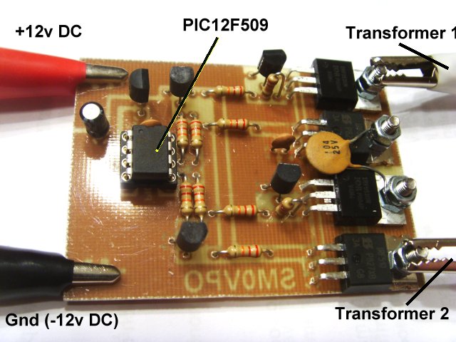
The prototype unit looks like this, but this was before I added the 50/60Hz switching. This I have tacked on the back of the prototype board. The PCB I supply will incorporate the 50/60Hz resistor, R1, and the 330 Ohms "be-kind-to-the-regulator" resistor.
Have fun, but remember that high voltages can kill, even those coming from a micro-computer.
Return to start page