Enhancement mode means that the FET must be biased on to set the operating point for use as an amplifier (much like biasing a bipolar transistor).
Depletion mode means that it must be reverse biased, or biased off, to set the operating point (as in a valve amplifier).
The junction FET or JFET operates in the depletion mode and to reverse bias a JFET stage, it is only necessary to insert an appropriate value of resistance in series with the source electrode (much like cathode bias in a valve stage).
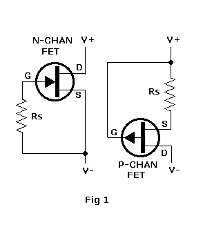
Figure 1 shows a P channel JFET and an N channel JFET, each with a source bias resistor Rs.
The only difference between the two circuits is the polarity in connecting to the supply rail.
Voltage is developed across Rs and applied the gate-to-source junction in reverse or depletion polarity.
Due to the reverse feedback, the drain current is stabilised at a value determined by the value of Rs.
Now instead of Rs in the P channel JFET, lets replace it with the source and drain of the N channel JFET, and instead of Rs in the N channel JFET lets replace it with the source and drain of the P channel JFET.
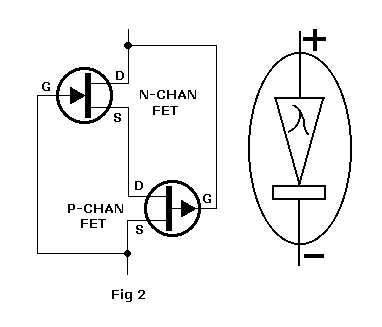
Now we get the circuit of Fig 2 and this is our Lambda circuit.
Connected in this way the two transistors interact with each other an produce the "negative-resistance" characteristic or backward bending curve.
This is well known in the Tunnel diode and the Tetrode vacuum tube.
Because of the similarity of the Greek character LAMBDA to the shape of the "neg-resistance curve" the term Lambda-Diode was coined to describe the circuit element under discussion.
To make a negative resistance oscillator we simply connect a tuned circuit in series with the Lambda circuit and the drain to source supply and set the supply voltage to a suitable level for oscillation to occur.
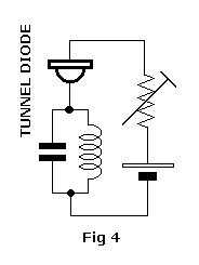
The advantage of this type of oscillator is that two-terminal (i.e. no taps) inductance coils are all thats needed!
Since P-channel JFETS have a relativley shallow transfer curve, a bipolar transistor can be used in its place.

The circuit shown is that of a "gate-dip" oscillator, used to determine the resonant frequency of parallel LC circuits.
FET T1 and the bipolar transistor T2 form the Lambda diode.
The "Lambda-diode" so formed is biased to the negative resistance region by means of P1 .
Experimentation would suggest that point is about 4 volt.
(In a tunnel diode this point is about 1 volt).
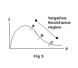
The Lambda diode curve can be plotted at your test bench and by considering the neg-resistance region A-C: a resistance value of approx 600 ohm is obtained by taking the ratio of voltage change to current change for "A-C" curve section.
From the point of view of RF currents: the base of T2 is connected to the drain of T1 and the gate of T1 is connected to the collector of T2 (via 47pF capacitor).
With the wiper of P1 most +ve oscillator is inoperative and meter reading will be at a minimum.
The oscillator will work provided that the shunt resistance of the resonant circuit is at least greater the the -ve resistance value of the lambda diode.
This we established earlier as being about 600 ohm.
Even low-Q tuned circuits can have a high shunt resistance which means that the circuit oscillates so freely it can be hard to pick up the dip even when the test LC network is being "dipped".
Therefore advance P1 wiper till deflection just increases (oscillator is now running).
Also the shunt resistance of the LC circuit may be artifically lowered (by paralleling with a fixed resistor of approx 1.6K to 4.7K - Higher freq' least resistance - see table).
This allows this (very efficient) oscillator to operate with just enough feedback to produce a reliable output, and hence when used as a Dip-meter,
the "dip" phenomina will be more evident and not masked by the ability of the Lambda oscillator to produce full output even with a Low Q tuned circuit and the proximity of a nearby test LC network trying to absorb some RF energy!
REFERENCES:
Wireless World: Jan & Feb 1957 M G Scroggie (Cathoderay)
NEGATIVE RESISTANCE - MYSTERY OF THE BACKWARD BENDING CURVE
Elektor magazine October 1979. A modern grid-dip meter page 10-22
Amateur Radio (Australia) January 1997 A dip meter using the Lambda diode page15