| www.play-hookey.com | Tue, 08-19-2003 | |
| Digital | Logic Families | Digital Experiments | Analog | Analog Experiments | DC Electronic Theory | Optics | Computers | Semiconductors | Test HTML | ||
| Bistable Multivibrator with NOR Inputs |
|---|
The basic bistable multivibrator we examined in the last experiment has a basic shortcoming: there are no external inputs to this circuit. After all, we can't very well use grounding wires in a digital circuit to get it to change states at specific times. We need to apply external input signals in a standard manner.
Since we are basically using RTL inverters to create the multivibrator, the obvious approach is to convert the inverters into NOR gates, and apply the input signals to the additional inputs. This would cause this circuit to behave just like the RS NOR latch demonstrated in one of the interactive pages on this site.
In this experiment, we will ad the components necessary to turn the basic bistable multivibrator into an RS NOR latch circuit.
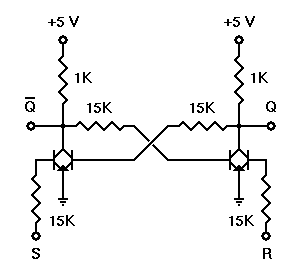
The circuit for the NOR version of the bistable multivibrator requires only that we add a transistor and input resistor to each of the two inverters already present, thus transforming them into 2-input NOR gates.
Note that we have now labeled the inputs and outputs using the standard latch nomenclature. It doesn't really matter which transistor you designate as the Q output, so long as you remain consistent with all input and output assignments. Thus, the designations here are strictly arbitrary.
To construct and test the RS NOR latch circuit on your breadboard, you will need the bistable multivibrator circuit you constructed in the previous experiment, plus the following experimental parts:
The parts for this experiment will be mounted on the lower half of the breadboard socket, just below the parts remaining from your previous experiment. If you have not yet performed the previous experiment, go back now and complete it. Then refer to the image and text below and install the parts as shown.


Click on the `Start' button below to begin. If at any time you wish to start this procedure over again from the beginning, click the `Restart' button that will replace the `Start' button.
Remove the black grounding jumper you used in the last experiment. Put it aside for use in future experiments.
Click on the image of the jumper you just removed to continue.
Prepare a 0.3" black jumper (or use one left over from earlier experiments), and install it in the location indicated to the right.
Click on the image of the jumper you just installed to continue.
Locate or prepare a second 0.3" black jumper, and install it in the location indicated in the assembly diagram.
Again, click on the image of the jumper you just installed to continue.
Prepare a 0.3" white jumper and install it in the location indicated to the right.
As before, click on the image of the jumper you just installed to continue.
Prepare a second 0.3" white jumper and install it in the location indicated to the right.
Once more, click on the image of the jumper you just installed to continue.
Locate a 15K, ¼-watt resistor (brown-green-orange) and form the leads to a spacing of 0.5". Clip the formed ends to a length of ¼", and install the resistor as shown in the assembly diagram.
Click on the image of the resistor you just installed to continue.
Locate another 15K, ¼-watt resistor (brown-green-orange) and form the leads to a spacing of 0.5". Clip the formed ends to a length of ¼", and install the resistor as shown to the right.
Again, click on the image of the resistor you just installed to continue.
Locate a 2N3904 or 2N4124 NPN switching transistor and form its leads to fit 0.1" spacing. Install this transistor in the location shown to the right. Be careful to observe the orientation of the transistor; the emitter must be connected to the black grounding jumper.
Click on the image of the transistor you just installed to continue.
Locate another 2N3904 or 2N4124 NPN switching transistor and form its leads to fit 0.1" spacing. Install this transistor in the location shown to the right. Be careful to observe the orientation of the transistor.
Again, click on the image of the transistor you just installed to continue.
Locate a 6" orange jumper left over from previous experiments. If necessary, cut a 6" length of orange hookup wire and remove ¼" of insulation from each end. Connect one end of this jumper to the location shown in the assembly diagram. Connect the other end to logic switch S0.
Click on the image of the jumper you just installed to continue.
Locate or prepare a second 6" orange jumper, and connect one end to the location shown to the right. Connect the other end to logic switch S1.
Once more, click on the image of the jumper you just installed to continue.
This completes the construction of your experimental circuit. Check your assembly carefully against the figure to the right, and correct any errors you might find. Then, proceed with the experiment on the next part of this page.
Set S0 to logic 1 and S1 to logic 0, and turn on power to your experimental circuit. Then set S0 to logic 0. Assuming that the latch is now in its reset state (Q output is logic 0), which LED monitors the Q output, and which one monitors the Q' output?
Set S1 to logic 1, then back to logic 0. What is the effect of this action? Now set S0 to logic 1 and then back to logic 0. Did you get the result you expected? Repeat these actions a few times. Based on your results, which switch corresponds to the R input, and which one to the S input?
Set both S0 and S1 to logic 1. How does your experimental circuit respond to this? What can you say about setting both inputs to logic 1 this way?
When you have made your determinations, turn off the power to your experimental circuit and compare your results with the discussion below.
You should have found that the circuit for this experiment behaved exactly like the interactive demonstration of the RS NOR latch circuit. Since you had S0 set to logic 1 when you turned power on, L0 was off and L1 was on. We defined this as the reset state of the latch circuit, so L0 shows the state of the Q output, while L1 shows the state of the Q' output.
From the schematic diagram of this circuit, as well as from the fact that we started with S0 at logic 1, we can infer that S0 provides the R input signal, while S1 provides the S input signal. You proceeded to verify these assumptions, by demonstrating that S1 caused the latch circuit to switch states to turn L1 off and L0 on (the Set state), while S0 turned L1 on and L0 off (the Reset state).
Applying further S0 signals while L0 was off had no effect, and applying S1 while L0 was on had no effect. In each case, the latch was already in the state called for by that switch, so no further change took place. This is the normal behavior of this type of latch circuit, and again matches the behavior of the interactive demonstration.
When you have completed this experiment, make sure power to your experimental circuit is turned off. Remove all of the experimental components and put them aside for future use. You'll use many of them in the next experiment.
| Your next experiment is: Monostable Multivibrator |
|---|
| All pages on
www.play-hookey.com copyright © 1996, 2000-2003 by Ken Bigelow Please address queries and suggestions to: webmaster@play-hookey.com |